Browse categories
Explore
Fiverr Pro
English
$
USD
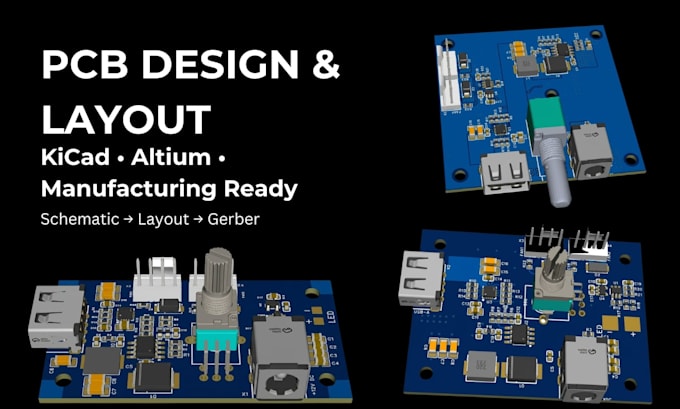
I will design a clean, practical and manufacturing-ready PCB layout from your schematic or circuit requirements.
I work on custom electronics boards including embedded systems, sensor boards, controllers, IoT hardware and other electronic products. Depending on the package, I can provide PCB layout, component placement, routing, design-rule checks, Gerber files, BOM, 3D board views and editable source files.
I can work with KiCad or Altium Designer.
My approach is engineering-focused: the board should not only look correct on screen, but also be practical to manufacture, assemble, test and develop further.
Typical work includes:
For complex boards, RF/high-speed designs, unusual power requirements or projects with incomplete documentation, please message me first so I can review the scope and provide the correct package or a custom offer.
Send the schematic, board requirements and any mechanical constraints you already have.

Can you design a PCB from my existing schematic?
Yes. If your schematic is complete and the component information is available, I can convert it into a PCB layout, place and route the components, run the appropriate design checks and prepare the required manufacturing files.
Can you create the schematic as well?
Yes, but schematic development is outside the standard PCB layout package. If you only have a circuit idea, block diagram or functional requirements, send them to me first and I can review the scope and provide a custom offer where appropriate.
Do you work with KiCad and Altium Designer?
Yes. I can work with KiCad or Altium Designer depending on the project requirements and the source files available.
Will I receive Gerber files?
Yes. Gerber and other manufacturing outputs are included where they are part of the selected package.
Will I receive the editable source files?
Yes, editable project/source files are included according to the selected package.