Browse categories
Explore
Fiverr Pro
English
$
USD
pcb design
I will design a custom 4-layer flexible PCB for compact embedded devices, wearable electronics, IoT products, sensors, and space-constrained electronic assemblies.
What I can design:
What you will receive:
I focus on compact layouts, practical flex-circuit design considerations, reliable routing, and clear manufacturing documentation tailored to your device.
Please message me before placing an order so we can confirm your requirements and project scope.
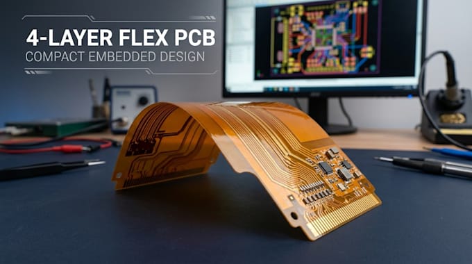

Can you design a complete four-layer flexible PCB?
Yes. I can prepare a four-layer flex layout based on your circuit, mechanical requirements, layer stackup, and manufacturing constraints.
Can the design fit a compact embedded device?
Yes. I can optimize component placement and routing for restricted board dimensions, connector locations, and available enclosure space.
Can you account for bending requirements?
Yes. I can account for the specified bend radius and bend locations. Dynamic flexing requires additional attention to copper geometry, materials, and expected cycle life.
Can you use polyimide material?
Yes. Polyimide-based flex construction can be considered according to the selected manufacturer's available materials and stackup options.
Can you route high-speed signals on a four-layer flex PCB?
Yes, subject to the design requirements and fabrication capabilities. Impedance control, dielectric properties, reference layers, and connector transitions must be considered.
Will you provide manufacturing files?
Yes. The agreed package can include Gerber files, drill files, BOM, and editable PCB design files.
Does the service include fabrication and bend-cycle testing?
Not by default. Manufacturing, assembly, and physical reliability testing can be arranged separately if they are within the agreed project scope.
