Browse categories
Explore
Fiverr Pro
English
$
USD
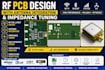
Professional RF PCB Design for IoT and Wireless Systems
I will create RF PCB designs with antenna integration and impedance tuning for IoT devices, wireless communication systems, Bluetooth, WiFi, LTE, and 5G applications.
I specialize in designing high frequency circuits that ensure excellent signal integrity, controlled impedance, and minimal noise or interference, which are critical for reliable RF performance.
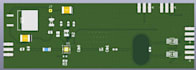
With strong expertise in RF PCB layout and antenna optimization, I deliver production-ready designs that are optimized for real-world functionality and manufacturability.
I work on both schematic understanding and full PCB layout development, ensuring your project is well structured from concept to fabrication.
I use professional industry tools such as Altium Designer, KiCad, CST Studio Suite, and HFSS for RF simulation, antenna tuning, and circuit optimization, including analysis of return loss, S-parameters, and impedance matching.
What I will deliver:
Complete RF PCB layout ready for fabrication
Antenna integration and tuning support
Controlled impedance routing for RF signals
Simulation and performance optimization (if required)
Gerber files, BOM, and production documentation
Dm me before ordering