Browse categories
Explore
Fiverr Pro
English
$
USD
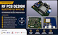
Professional RF PCB Design for IoT and Wireless Systems
I provide professional RF PCB design services for Bluetooth, WiFi, and 5G applications, focusing on high performance wireless connectivity and robust signal integrity.
I design reliable RF circuits with careful attention to impedance matching, transmission line control, and EMI/EMC reduction to ensure stable operation in real world conditions.
My work covers complete PCB development from schematic capture to production ready files, optimized for low noise, high speed operation, and efficient power handling.
Whether its compact IoT devices, wireless communication modules, or advanced RF systems, I ensure your design meets industry standards and manufacturing requirements.
What you will get:
RF schematic design and PCB layout
Controlled impedance routing and stack up design
Antenna design and matching network optimization
Gerber, BOM, and fabrication ready files
DFM checks for manufacturability
Optional RF simulation support (HFSS, ADS, CST)
Software used: Altium Designer, KiCad, Cadence OrCAD, CST Studio Suite, Keysight ADS, MATLAB, and LTspice for simulation and RF analysis.
Dm me before ordering