Browse categories
Explore
Fiverr Pro
English
$
USD
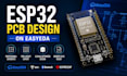
Smart, Robust, and Scalable PCB Design for Industrial Applications
I am a professional PCB de_sign engineer specializing in ESP32-based circuit de_sign and PCB layout using EasyEDA. I help turn your ideas into clean, functional, and manufacturing-ready PCB de signs for prototypes and real-world applications.
Whether you need an IoT device, smart controller, or embedded system, I will design a complete solution including schematic and PCB layout optimized for performance and reliability.
My goal is to deliver clean, well-routed, and production-ready PCB de signs that are easy to manufacture and work reliably in real applications.
️ What I Offer
Expertise
Why Choose My Service
Contact Me First To Talk


Specialization:
Circuit design
•
Schematics
•
Gerber
File format:
Gerber
•
STEP
•
VRML
•
BRD
•
ODB
Software:
Altium Designer
•
EasyEDA
•
LabVIEW
•
PSIM
•
AutoCAD
•
PSpice
Interface:
HDMI
•
TDM
•
UART
•
SDIO
•
PCIe


