Browse categories
Explore
Fiverr Pro
English
$
USD
PCB Design Engineer, Schematic Layout and Gerber Files
Need a custom IoT PCB or a professional PCB layout for your wireless electronics project?
I will help turn your IoT hardware requirements or existing circuit schematic into a custom PCB design using KiCad.
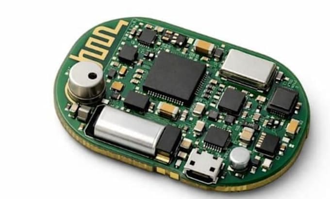
I focus on practical PCB layout, component placement, routing, and wireless module integration for embedded electronics projects.
MY SERVICES
BEFORE ORDERING
Please provide your circuit schematic if available, preferred components or wireless module, board dimensions, and required output files.
If you only have an idea rather than a complete schematic, contact me first so we can confirm what is feasible and agree on the scope.
THANK YOU;
What do you need to start my PCB design project?
I need your project requirements, circuit schematic (if available), preferred components, board dimensions, and required output files.
Can you design IoT PCBs using ESP32?
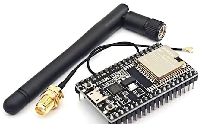
Yes, I can help with ESP32-based PCB layout and compatible wireless module integration, depending on your project requirements.
Which PCB design software do you use?
I use KiCad for schematic-related work, PCB layout, routing, and design file preparation.
. Will I receive Gerber files and a BOM?
Yes, Gerber files, drill files, and a Bill of Materials (BOM) are available according to your selected package.
Can you work with an existing schematic?
. Yes, I can create a PCB layout from your existing schematic, provided the design is suitable and the requirements are clear.
Do you design wireless and RF PCBs?
I provide PCB layout and integration of compatible wireless modules. Advanced RF circuit design, antenna tuning, and RF testing are not included unless agreed upon separately.