Browse categories
Explore
Fiverr Pro
English
$
USD
I design PCBs that work in the real world, not just look clean on screen.
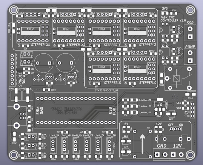
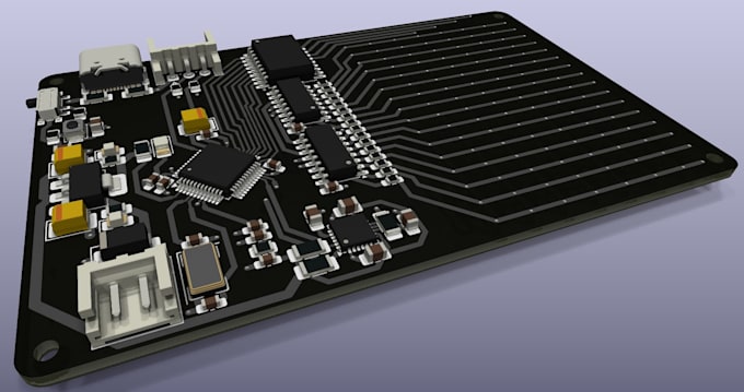
I'm a Mechatronics Engineering graduate with hands-on PCB experience across real, physical projects not just tutorials. My capstone project, FabX, was a desktop PCB fabrication machine where I designed the control board myself: sizing tracks for full system current draw, and implementing protection circuitry (Schottky diodes, fuses, optocoupler isolation). I've also designed sensor-heavy boards for competition robotics (Micromouse), integrating IR sensors, IMU, encoders, and power regulation on a tightly constrained footprint.
What I can do for you:
Send me your requirements and I'll get back to you with a realistic timeline. Let's build something that survives real use.



Specialization:
Circuit design
•
Schematics
•
Layout
•
Footprint
•
Gerber
File format:
Gerber
•
STEP
•
Software:
Fusion 360
•
KiCad
Interface:
UART
•
USB
•
SPI
•
I2C