Browse categories
Explore
Fiverr Pro
English
$
USD
PCB EXPERT
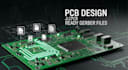
pcb design pcb layout gerber bom jlcpcb fabrication ready pcb files.
This gig focuses on creating pcb layout and gerber manufacturing files specifically optimized for JLCPCB fabrication services.
If you already have a schematic or circuit idea, I will convert it into clean pcb layout routing and generate fabrication-ready gerber files compatible with JLCPCB manufacturing standards.
Services included:
pcb layout design
gerber file generation
bom creation
manufacturing ready pcb files
electronics pcb board layout
Your files will be organized and ready to upload directly to JLCPCB fabrication platform without design errors.
Tools used:
kicad
easyeda
altium designer
This service is suitable for:
prototype pcb boards
electronics hobby projects
product development pcb boards
manufacturing ready pcb designs

What files will I receive
You will receive gerber files ready for jlcpcb manufacturing, schematic files, and source design files.
Can the PCB be uploaded directly to JLCPCB
Yes. The gerber files are exported according to jlcpcb fabrication requirements.
Which software do you use
kicad easyeda and altium depending on the project needs.
Can you edit or fix my existing pcb
Yes, existing pcb layouts and schematics can be reviewed and improved
Can you create bom files
Yes, bom files can be provided for component sourcing.
