Browse categories
English
$
USD
Connect to your AI
Electronics Engineer l PCB Design Expert
Stuck with obsolete electronics, missing design files, or discontinued parts? Relying on legacy hardware without digital blueprints risks production downtime and manufacturing failure. You need precise reverse engineering executed to modern production standards.
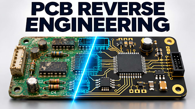
I provide premium PCB reverse engineering, Gerber-to-schematic reconstruction, and outdated hardware modernization services. I translate your physical board photographs, old manufacturing files, or scanned paper schematics into fully editable, modern EDA design packages.
What my professional engineering services include across packages:
Schematic Reconstruction: Recreating lost electrical logic maps into clean, structured digital schematics.
PCB Clones & Layout Replicas: Re-routing physical boards track-for-track into modern CAD layouts.
Component Swaps & Upgrades: Replacing obsolete microcontrollers with active modern equivalents.
Supported EDA Tools: Altium Designer, KiCad, Eagle, and EasyEDA.
Note: Complex multi-layer boards require manual review. Message me with clear photos of both sides of your board or order the Basic Board Audit so we can map out your exact cloning scope!

What software formats do you deliver the reconstructed files in?
I deliver fully organized, modern native source files in Altium Designer, KiCad, or EasyEDA, alongside standard manufacturing outputs including complete Gerber files and updated Bills of Materials (BOM).
Can you reverse engineer a PCB layout just from clear photographs?
Yes, for 1-layer and standard 2-layer boards, clear, flat, high-resolution photographs of both the top and bottom sides are often enough to trace the circuitry and recreate the exact design files.
