Browse categories
Explore
Fiverr Pro
English
$
USD
PCB design and embedded systems engineer
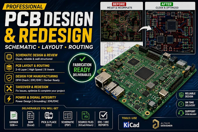
Need an existing PCB design reviewed, redesigned, or taken from an unfinished state to a manufacturing-ready board?
I can help with PCB schematic design, PCB layout, routing, redesign, design review, EDA migration, and manufacturing preparation for electronics projects ranging from simple boards to complex embedded systems.
Services include:
I can also take over unfinished or problematic PCB projects and help correct routing, design, or workflow issues.
Send me your files and requirements before ordering so I can review the scope and recommend the right package.
Can you take over an unfinished PCB?
Yes. I can review the existing design and continue or redesign it as required.
Can you migrate my PCB to another EDA platform?
Yes, depending on the source files and project condition.
Do you provide Gerbers?
Yes, for packages that include manufacturing files.
Can you provide BOM and pick-and-place?
Yes.
Can you redesign an existing PCB?
Yes. I can review the existing design and correct issues within the agreed scope.
Do you design multilayer PCBs?
Yes, including 2–6 layer designs.
Can you handle high-speed routing?
Yes, where the project requirements call for it.
Do you manufacture the PCB?
The gig focuses on engineering and design. Physical manufacturing is separate.
