Browse categories
Explore
Fiverr Pro
English
$
USD
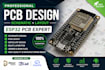
PCB Designer and Web Developer, Hardware and Digital Done Right
Your PCB schematic looked perfect. Then you sent it to the factory and the ground plane was missing, the RF trace was a mess, and your ESP32 module smoked on first power-up . That is the gap between theory and a board that actually works. I bridge that gap.
Most pcb design projects fail in the silent details: port labels obscured by symbols, ground symbols pointing sideways, signal flow running backward, and DRC checks that pass while the board still breaks . I have reviewed enough first-time ESP32 PCB design attempts to know where the traps hide. Missing line checks after wiring in Altium. Via sizes that default wrong. Copper pours that become dead copper because of a forgotten keepout layer . I catch these before your board becomes an expensive coaster.
What I deliver:
If your last board came back broken or your schematic is a maze of dashed lines and overlapping text, message me. I turn chaos into a board that powers up and stays up.