Browse categories
Explore
Fiverr Pro
English
$
USD
PCB Embedded and Firmware Development
HELLO THERE,
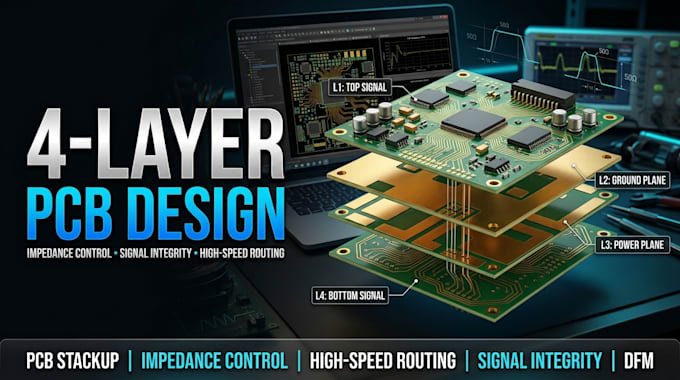
I will design a 4 layer PCB engineered for controlled impedance, high speed signal integrity, and reliable manufacturability. My design approach focuses on stack up engineering, return current continuity, reference-plane integrity, differential pair routing, and noise reduction to support demanding digital and mixed-signal applications.
What I Provide:
Why Choose Me?
Ready to move your PCB from concept to fabrication? Send your schematic, interface requirements, and board constraints so I can define the appropriate stack up and routing strategy for your project.
Can you design a complete 4 layer PCB from my schematic?
Yes. I can develop the component placement, routing, copper planes, design rule checks, and fabrication outputs based on your schematic and project constraints.
Can you design controlled-impedance traces?
Yes. I can design for specified single-ended and differential impedance targets using the relevant dielectric properties, copper thickness, trace geometry, and manufacturer stackup information.
Do you support high speed interfaces such as USB and Ethernet?
Yes, depending on the interface and design complexity. I can apply suitable routing constraints, differential pair rules, reference plane continuity, and length matching where required.
Which PCB design software do you use?
The project can be handled in a compatible PCB CAD tool, such as Altium Designer or KiCad, depending on the agreed workflow and the source files you provide.
Will you provide Gerber and manufacturing files?
Yes. The agreed package can include Gerber, NC drill, BOM, pick-and-place, and other required manufacturing outputs.
Can you guarantee that my PCB will work perfectly on the first fabrication?
No responsible designer can guarantee that without complete requirements and physical validation. I can perform design checks and follow sound layout practices to reduce avoidable electrical and manufacturing risks.