Browse categories
Explore
Fiverr Pro
English
$
USD
PCB Engineer, Firmware Developer And RF, IoT, Hardware And Reverse Engineering
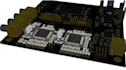
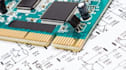
I will engineer RF multilayer PCB layouts, schematic circuits, impedance controlled routing, and antenna designs using Altium Designer. I specialize in high frequency PCB design with proper signal integrity, impedance matching, and EMI considerations. From RF circuits to complex multilayer boards, I deliver precise, optimized, and manufacturing-ready Gerber files. Whether for IoT, wireless, or communication systems, you will get reliable, production-ready PCB solutions built for performance and stability.
What You'll Get:
Why Choose Me:
Message me now to engineer your RF PCB with precision and performance!
Do you design RF and high frequency PCBs?
Yes, I specialize in RF PCB design with impedance control and signal integrity optimization.
Which software do you use for RF PCB design?
I primarily use Altium Designer for advanced PCB and RF layout development.
Can you design antennas for PCB projects?
Yes, I design and optimize PCB antennas for wireless and communication systems.
Will my PCB be ready for manufacturing?
Yes, I provide complete Gerber files and documentation ready for production.
Do you support multilayer and high speed designs?
Yes, I handle multilayer PCBs with controlled impedance and high-speed routing.


