I will review pcb design fix layout errors and troubleshoot hardware

United States

I speak English, French, German

High Quality PCB Design for Every Project

I'm a professional electronics engineer specializing in high-density, multi-layer PCB design and layout. I transform your concepts and schematics into production-ready circuit boards using industry-le...
About this Gig

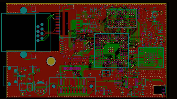
This engineering service conducts independent design verification on user-submitted PCB databases. The objective is the identification of layout discrepancies, schematic mismatches, and structural violations prior to manufacturing release. Native project files from Altium Designer, KiCad, or Cadence Allegro are subjected to manual and automated constraints auditing.


Verification Matrix:

  • Netlist Integrity: Verification of schematic-to-layout synchronization, pin mappings, and component footprint pin-outs against official manufacturer datasheets.
  • Signal & Power Audits: Analysis of high-speed trace return paths, differential pair phase matching, current density via counts, and DC power distribution constraints.
  • DFM / DFA Analysis: Inspection of copper-to-edge clearances, aspect ratios, solder mask dams, and component clearances relative to commercial fabrication capabilities.


Deliverables:

All assessments conclude with an actionable technical markdown report mapping specific design vulnerabilities and required corrective modifications. Advanced tiers include direct database remediation and updated Gerber X2 production file generation.


Contact me before ordering!

Specialization:

Circuit design

Schematics

Layout

Footprint

File format:

Gerber

STEP

VRML

SCH

PDF

Software:

Allegro

Altium Designer

Cadence OrCAD

Eagle CAD

EasyEDA

Interface:

HDMI

MIPI DSI/CSI

I2S

TDM

UART

USB

SPI

I2C

SDIO

PCIe

Wi-Fi

BLE