Browse categories
Explore
Fiverr Pro
English
$
USD
PCB Design and Embedded System
HELLO AND WELCOME TO MY GIG!!
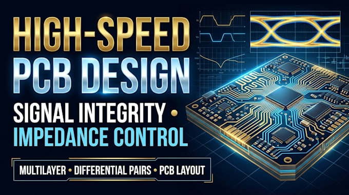
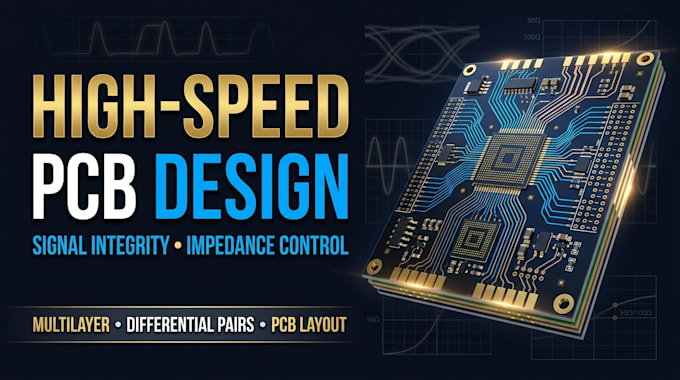
High speed PCB design requires precise routing, signal integrity, controlled impedance, and stackup planning for reliable performance. I provide professional PCB design and layout for advanced digital electronics, embedded hardware, and multilayer boards, focusing on differential pair routing, length matching, transmission lines, crosstalk reduction, return-path optimization, and power integrity.
WHAT I OFFER,
WHY CHOOSE ME?
Whether you need a new high speed PCB or an existing layout optimized, I tailor each design to your technical requirements and manufacturing constraints.
Kindly share your project details to get started!
MESSAGE ME NOW !!!!!!
What is high speed PCB design?
High speed PCB design focuses on routing fast digital signals while managing impedance, reflections, crosstalk, timing, and return paths.
Can you design a PCB with controlled impedance?
Yes, according to the agreed impedance targets, stackup, material properties, geometry, and fabrication constraints supplied for the project.
Do you support differential pair routing?
Yes. Depending on the interface, the layout can include differential-pair spacing, length matching, skew control, and reference-plane considerations.
Which high-speed interfaces can you support?
Project-dependent support can include DDR, PCIe, USB, Ethernet, LVDS, HDMI, and other high-speed digital interfaces. Kindly provide the exact interface and revision.
Can you work with an existing PCB?
Yes. Existing designs can be reviewed for routing improvements, impedance planning, return-path continuity, layout corrections, and design-rule issues.
Which deliverables do you provide?
Depending on the selected package, deliverables can include PCB source files, Gerber files, drill files, BOM, pick-and-place data, and design-rule reports.
Is signal-integrity simulation included?
Simulation is included only when agreed in the package or custom offer. The required models, interface specifications, stackup, and simulation tools must be available.
Can you guarantee that my PCB will pass signal-integrity testing?
No unconditional guarantee is appropriate without complete system information and validation. Results depend on the design, components, fabrication, assembly, and testing conditions.