I will develop high speed rf pcb layout with emi and signal integrity optimization

United States

I speak English

HighSpeed RF PCB Design Engineer

I design circuit boards that handle high-speed data and radio frequencies without crashing or dropping signals. I focus on the physics of the board to make sure it actually passes certification. I bel...
About this Gig

WELCOME TO MY GIG,

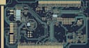
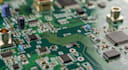
I am a professional PCB Designer and Electronics Engineer specializing in high-speed and RF PCB layout with strong expertise in signal integrity and EMI optimization.

I will develop high-speed RF PCB designs that ensure reliable performance, minimal noise, and efficient signal transmission for your project.


What I offer:

  • High-speed RF PCB layout (28+ layers)
  • Controlled impedance routing & differential pairs
  • Signal integrity (SI) optimization
  • EMI/EMC reduction techniques
  • Component placement and stackup guidance
  • Manufacturing-ready Gerber files


Why choose me?

  • Experience with RF and high-speed systems
  • Industry-standard tools (Altium, KiCad, etc.)
  • Clean, production-ready designs
  • Fast communication and support


Whether you're building IoT devices, wireless systems, or advanced electronics, Ill help you achieve a stable and optimized PCB design.

Specialization:

Circuit design

Schematics

Layout

Footprint

File format:

Gerber

STEP

VRML

BRD

3DS

Software:

Allegro

Altium Designer

Cadence OrCAD

DipTrace

Eagle CAD

Interface:

HDMI

MIPI DSI/CSI

I2S

TDM

UART

USB

SPI

I2C

SDIO

PCIe

Wi-Fi

BLE