Browse categories
English
$
USD
Connect to your AI
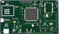
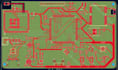
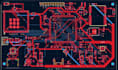
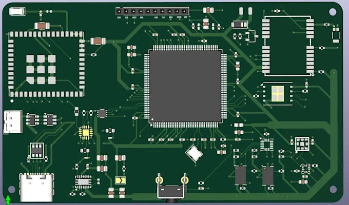
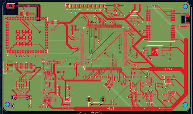
I will design rf pb layout, antenna circuits, high frequency and wireless boards
Precision 3D CAD Modeling for Product Design and Manufacturing
I'm a professional CAD Designer with expertise in 3D CAD Modeling, Product Design, Mechanical Design, Reverse Engineering, 3D Printing Design, and Manufacturing-Ready Engineering Solutions. I use Soli...
Level 1
Has met certain performance criteria and shows strong potential in the marketplace.
About this Gig
Need an RF PCB design that handles high frequency signals without poor routing, interference or costly redesigns?
I can turn your circuit idea, schematic or reference into a clean, manufacturing-ready RF PCB layout.
I offer RF PCB design for wireless electronics, antenna circuits, IoT devices and high frequency applications, with attention to impedance, grounding, shielding and signal integrity.
WHAT I OFFER:
- RF PCB layout and schematic
- High frequency PCB design
- 50 ohm impedance routing
- RF antenna PCB layout
- WiFi and Bluetooth PCB
- 2.4 GHz antenna circuits
- LoRa and LoRaWAN PCB
- 433 MHz and 868 MHz RF PCB
- RF transmitter and receiver PCB
- RF transceiver PCB
- GPS and GNSS PCB
- RF amplifier and LNA PCB
- RF filter and matching networks
- ESP32 and STM32 wireless PCB
- Zigbee and BLE PCB
- Microstrip and CPW routing
- RF grounding and shielding
- RF PCB redesign and DFM
- Gerber, BOM and assembly files
WHY CHOOSE ME?
Clear communication, careful RF layout and organized design files tailored to your requirements.
Message me before ordering to discuss your RF PCB project!