I will design hdi multilayer pcb for iot, rf, embedded systems, smart devices, hardware

United States

I speak English, French, Spanish, German, Portuguese

Electronics Engineer PCB Design for Power Electronics IoT and Wearable devices

I'm a professional PCB Design Engineer specializing in GaN & SiC power electronics, wearable PCB, HDI multilayer PCB, IoT systems, & embedded hardware design. I design high-quality schematics and PCB ...
About this Gig

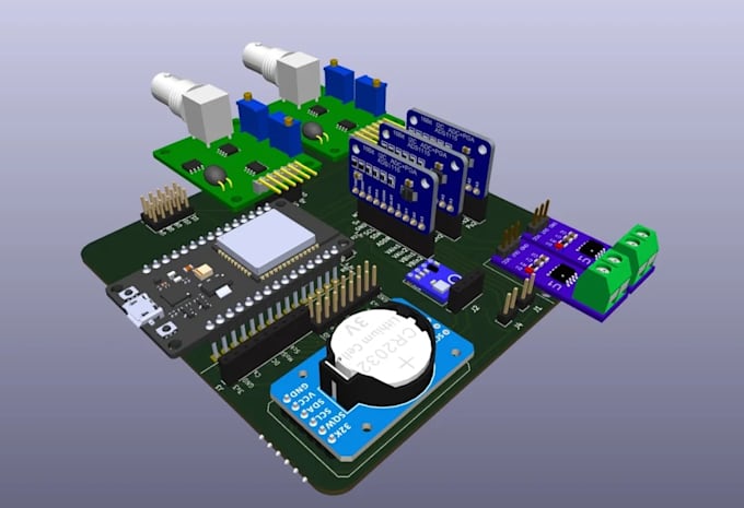
I will design professional HDI multilayer PCB for IoT, RF, embedded systems, smart devices, and AI hardware. I create compact, high-performance, manufacturing-ready PCB layouts with optimized signal integrity, EMI reduction, and reliable routing for wireless, automation, and smart electronic applications.


I use industry-standard tools such as Altium Designer, KiCad, EasyEDA, and Cadence OrCAD to ensure clean and production-ready PCB designs.


What I offer:

  • Schematic design and PCB layout
  • HDI multilayer PCB design
  • IoT and embedded system PCB
  • RF and wireless PCB routing
  • High-speed signal optimization
  • EMI and signal integrity optimization
  • Compact PCB layout for smart devices


Deliverables:

  • Gerber files
  • BOM (Bill of Materials)
  • Pick and Place files
  • PCB schematic files (SCH)
  • PCB source files
  • 3D PCB model (STEP file)
  • PDF documentation


Applications:

  • IoT devices and smart systems
  • RF and wireless communication devices
  • Embedded controllers and AI hardware
  • Automation and industrial electronics
  • Wi-Fi, BLE, GSM, and sensor devices


Contact me before ordering to discuss your project requirements and create a reliable PCB solution for your hardware product.

Specialization:

Circuit design

Schematics

Layout

Simulations

File format:

Gerber

STEP

SCH

PDF

ODB

Software:

Altium Designer

Cadence OrCAD

EasyEDA

Fusion 360

KiCad

Interface:

UART

USB

SPI

I2C

Wi-Fi

BLE

LTE

NB-IoT