Browse categories
Explore
Fiverr Pro
English
$
USD
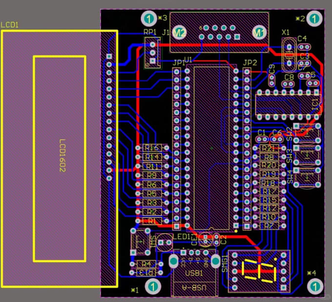
RF PCB DESIGNER AND ELECTRONIC ENGINEERING
Is your RF PCB suffering from weak WiFi range, antenna mismatch, unstable wireless connection, signal loss, EMI noise, or poor PCB routing?
You are in the right place.
I will help fix RF PCB antenna WiFi signal issues and improve wireless performance for your device, prototype, or product.
What I Offer:
RF PCB layout optimization
Antenna PCB design & tuning
WiFi / Bluetooth wireless PCB support
Signal integrity improvement
Impedance control routing
EMI / EMC noise reduction
PCB trace correction
Gerber file review & update
Schematic checking
Manufacturing ready files
Software I Use:
Why Choose Me:
Fast response
Clear communication
Reliable engineering support
Production ready results
Please message me before ordering for best project review.


Specialization:
Circuit design
•
Schematics
•
Layout
•
Gerber
•
Other
File format:
Gerber
•
BRD
•
SCH
•
3DS
•
Other
Software:
Allegro
•
Altium Designer
•
Cadence OrCAD
•
Eagle CAD
•
KiCad
What files do you need to start?
PCB files, schematic, Gerber, dimensions, and issue details.
Can you fix weak WiFi range?
Yes, I can review antenna placement, grounding, routing, matching, and layout problems.
Do you create new RF PCB from scratch?
Yes, from concept to production-ready PCB.
Which software do you use?
Altium, KiCad, EasyEDA, and related tools.
Do you provide Gerber files?
Yes, final manufacturing Gerber files can be included.
Should I message before ordering?
Yes, especially for custom or urgent jobs.