Browse categories
Explore
Fiverr Pro
English
$
USD
EasyEDA PCB Designer, PCB Layout and Circuit Schematic Engineer
Do you already have a circuit schematic but need a professional PCB layout?
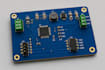
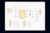
I will convert your circuit schematic into a clean, accurate, and manufacturing ready EasyEDA PCB layout. Whether your schematic is created in EasyEDA or provided as a PDF, image, or other supported format, I'll carefully transform it into an organized PCB design that follows good layout practices and is ready for fabrication.
Services Included
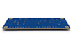
I focus on creating reliable PCB layouts with clean routing, proper component placement, and production ready outputs. Every project is completed with attention to detail, clear communication, and on time delivery.
Please contact me before placing your order to discuss your project requirements.
What schematic formats do you accept?
I can work with EasyEDA projects, PDF schematics, images, hand-drawn sketches (if clear), and other common schematic formats.
What files will I receive?
You'll receive the EasyEDA project files, PCB layout, Gerber files, BOM (if included), and other manufacturing-ready files according to your selected package.
Can you create a multilayer PCB?
Yes. I can design single-layer, double-layer, and multilayer PCB layouts depending on your project requirements.
Will the PCB be ready for manufacturing?
Yes. Every PCB layout is checked with DRC and prepared with manufacturing-ready Gerber files.
Do you use EasyEDA only?
Yes. This gig is dedicated to creating PCB layouts using EasyEDA, ensuring full compatibility with EasyEDA projects and PCB manufacturing workflows


