Browse categories
Explore
Fiverr Pro
English
$
USD
PCB Design Engineer, Custom PCB Layout, Schematics, Electronics Design
Is your PCB deslgn not working as expected?
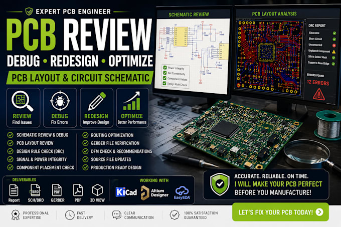
Do you need an experienced engineer to review, debug, redesign, or optimize your PCB before manufacturing? I can help identify deslgn issues, improve performance, and ensure your board is ready for production.
I specialize in PCB review, PCB debugging, circuit schematic analysis, PCB redeslgn, and layout optimization for embedded systems, IoT devices, automation hardware, and electronic products.
My services include:
PCB layout review and optimization
Circuit schematic debugging
Component placement optimization
Power and ground plane review
Gerber file verification
Manufacturing issue detection
PCB redesign and modifications
Whether your PCB has routing problems, electrical errors, manufacturing concerns, or performance issues, I will carefully analyze your deslgn and recommend the best engineering solution.
I work with KiCad, Altium Deslgner, and EasyEDA while following industry standard PCB design practices to improve reliability and manufacturability.
Please contact me before placing an order so we can discuss your deslgn files and project requirements.

What types of PCB issues can you identify?
I can review PCB layouts for routing errors, design rule violations, signal integrity concerns, power distribution problems, grounding issues, manufacturing risks, and component placement.
Which PCB software do you support?
I work with KiCad, Altium Designer, and EasyEDA. If your project uses another format, contact me before ordering.
Can you redesign an existing PCB?
Yes. I can modify or completely redesign your PCB while maintaining or improving its functionality.
Will you review my schematic as well?
Yes. I review both the schematic and PCB layout to ensure they are consistent and free from design issues.
Can you optimize my PCB for manufacturing?
Yes. I provide Design for Manufacturing (DFM) recommendations and verify that your design is suitable for PCB fabrication and assembly.
What files do I need to send?
You can send your PCB source files, schematic files, Gerber files, PDFs, or any project documentation you have. I'll review them and recommend the best approach.
Do you provide a report of the issues you find?
Yes. The Basic and higher packages include a clear explanation of identified issues and recommendations. Higher packages also include fixes and optimization where applicable.
Should I contact you before placing an order?
Yes. Every PCB project is different. Please contact me first so I can review your files and recommend the most suitable package.
