Browse categories
Explore
Fiverr Pro
English
$
USD
Hello there,
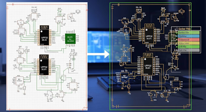
I specialize in component placement optimization, precise trace routing, multilayer PCB design, mixed signal layouts, differential pair routing, RF PCB layout, and power ground plane design. My designs follow strict DRC and DFM rules to ensure smooth fabrication and assembly.
I work with popular microcontrollers such as ATmega328P, ESP32, STM32, RP2040, and nRF52, and integrate analog interfaces
Services I Offer
What You Will Receive
You will receive a production-ready PCB design suitable for prototyping and mass manufacturing.


Can you convert my schematic into a PCB layout?
Yes, I convert schematics into optimized PCB layouts ready for manufacturing.
Do you design multilayer PCBs?
Yes, I design 2-layer to complex multilayer boards with proper stack-up planning.
Will I receive files ready for PCB fabrication?
Yes, you will receive Gerber files, BOM, and PCB source files.
Can you design PCBs for microcontrollers and IoT devices?
Yes, I design embedded PCBs for MCUs, IoT hardware, and wireless devices.
Do you optimize PCB layouts for compact size?
Yes, I specialize in compact and efficient PCB routing.