Browse categories
Explore
Fiverr Pro
English
$
USD
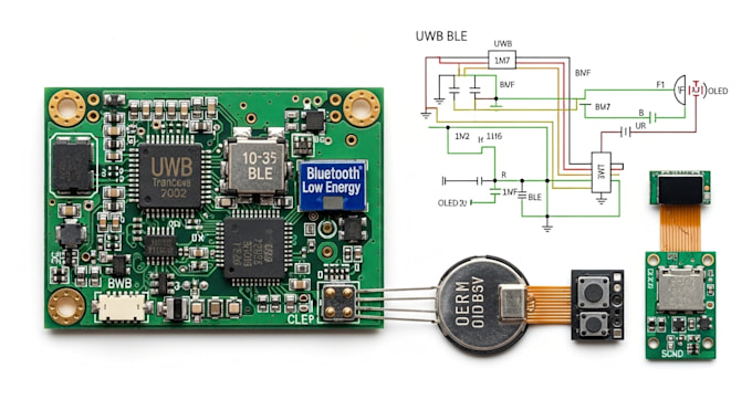
Are you developing a wearable device, IoT product, or RF hardware prototype using UWB or Bluetooth Low Energy (BLE)? I will design a professional schematic and compact PCB layout optimized for wearable electronics and low power devices.
This service is ideal for startup prototypes, smart gadgets, IoT devices, BLE products, and UWB tracking systems.
Services include:
What You Will Get:
Please contact me before placing an order so we can discuss your project requirements and ensure the best solution for your wearable device.


What information do you need to start the PCB design?
I need your project description, preferred components, PCB size limits, power requirements, and any reference schematic or block diagram.
Do you design wearable device PCBs?
Yes, I design compact PCBs optimized for wearable electronics with space and power constraints.
Can you integrate UWB and BLE modules?
Yes, I can integrate Ultra-Wideband (UWB) and Bluetooth Low Energy (BLE) modules with proper RF layout practices.
Do you design low-power circuits for IoT devices?
Yes, I specialize in low-power embedded hardware and IoT electronics.
What files will I receive after project completion?
You will receive schematic files, PCB layout, Gerber files, BOM, Pick & Place files, and assembly drawings.
Can you design PCBs ready for manufacturing?
Yes, all designs are optimized for manufacturing and prototype production.