Browse categories
Explore
Fiverr Pro
English
$
USD
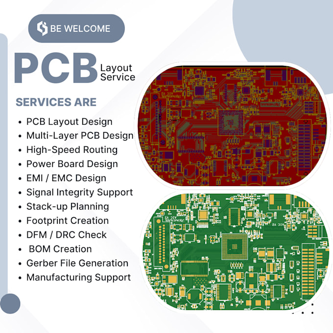
PCB LAYOUT DEIGNER
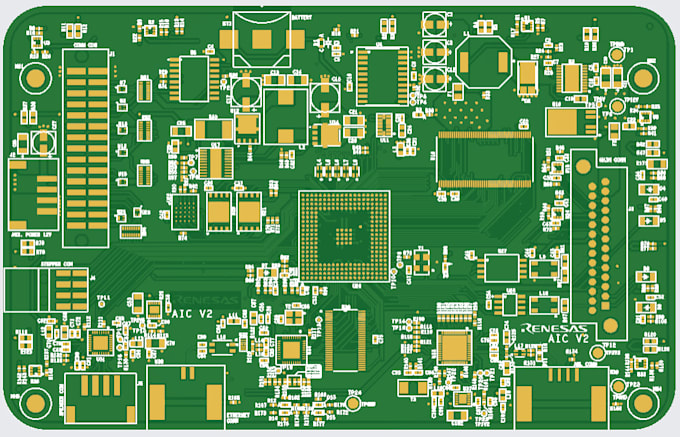
Hello, my name is Karthik and I am a professional PCB Design Engineer with experience in designing reliable and manufacturable printed circuit boards. I specialize in 1-layer, 2-layer, 4-layer and complex 6-10 layer PCB layouts. I focus on proper component placement, clean routing, power and ground optimization, and EMI/EMC-aware design to ensure stable circuit performance. I provide complete manufacturing outputs including Gerber files, drill files, BOM, and pick-and-place files. My goal is to deliver high-quality PCB layouts that are ready for production and meet industry standards. If you have a schematic or idea, I can convert it into a professional PCB design.


Specialization:
Schematics
•
Layout
•
Footprint
•
Gerber
File format:
Gerber
•
STEP
•
BRD
•
3DS
•
Software:
Allegro
•
Cadence OrCAD
•
EasyEDA
•
KiCad