Browse categories
English
$
USD
Connect to your AI
PCB Designer and Firmware Development
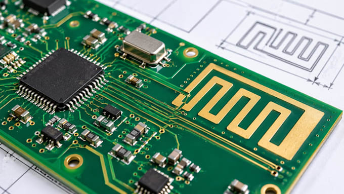
Are you experiencing poor wireless signal, low antenna efficiency or RF performance issues with your PCB?
I provide PCB antenna design and RF optimization services to help improve wireless performance, antenna placement and overall circuit efficiency.
Whether you are developing a WiFi, Bluetooth, IoT or other wireless device, I can help optimize your PCB antenna layout and RF characteristics.
What I offer:
I focus on practical design improvements to help address antenna performance issues and achieve better RF results.
Why work with me?
I pay attention to your PCB layout, antenna requirements and project specifications to provide solutions that suit your device and design goals.
Send me your PCB files and project requirements before ordering so we can discuss the best approach for your project.
Let's improve your PCB antenna and RF performance.
What files do you need to start?
I need your PCB design files, schematic (if available), antenna specifications and details about your wireless device.
Can you optimize an existing PCB antenna design?
Yes. I can review your existing antenna placement, ground clearance, impedance matching and RF layout to identify areas that need improvement.
Do you work with WiFi, Bluetooth and IoT antennas?
Yes. I can assist with PCB antenna optimization for WiFi, Bluetooth, IoT and other wireless applications.