Browse categories
Explore
Fiverr Pro
English
$
USD
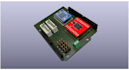
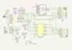
Need a professional PCB design for your project? Youre in the right place!
Im Kaustubh, an Electronics & Telecommunication Engineer with expertise in KiCAD and EasyEDA. I specialize in designing schematics, PCB layouts, and fabrication-ready files for everything from simple circuits to IoT devices, robotics boards, and wearables. My goal is to deliver clean, reliable, and manufacturable designs that save you time and cost during production.
What you get:
Schematic design & neat PCB layout
Gerber files for fabrication (JLCPCB, PCBWay, etc.)
Bill of Materials (BOM) with sourcing options
Design revisions to ensure accuracy
Advice on enclosure integration if needed
Packages:
Starter Circuit (Basic) 1-layer PCB for simple circuits/prototypes. Includes schematic + layout.
Pro Circuit (Standard) 1-layer PCB with revisions. Includes schematic, layout, Gerbers & BOM.
Advanced Circuit (Premium) 2-layer PCB with revisions. Includes schematic, layout, Gerbers, BOM & fab-ready files.
With experience in ESP32, STM32, Arduino, Teensy, and sensor-based systems, I ensure every design is practical and production-ready. Lets bring your circuit to life with a professional PCB tailored to your needs.