Browse categories
Explore
Fiverr Pro
English
$
USD
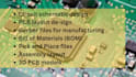
As a skilled Electronics and Electrical Design Engineer, I provide high-quality PCB de-sign services tailored to meet your exact project requirements. With strong expertise in embedded systems, product prototyping, circuit schematics, and PCB layout, I deliver reliable and production-ready de-signs.
I specialize in creating professional PCB layouts for microcontrollers, general electronics, and RF designs, including impedance-controlled routing for high-performance applications.
With over 5 years of experience using industry-standard PCB design tools, I can transform your idea into a complete schematic and fully functional PCBeven if you're starting with just a concept.
My Services Include:
Software Expertise:
Design Capabilities:
Every project is unique, so pricing packages are flexible based on your specific needs. Please contact me before placing an order


Can you design from scratch?
Yes, I can design the complete circuit schematic and PCB layout from scratch based on your concept or requirements.
Do you provide multi-layer PCB designs?
Yes, I design single-layer, double-layer, and multi-layer PCBs (up to 6 layers or more based on your project).
Can you handle RF or high-speed PCB designs?
Yes, I have experience with RF and high-speed designs, including impedance-controlled routing.
Will the design be ready for manufacturing?
Absolutely. All designs are checked with DRC/ERC and delivered as production-ready files compatible with PCB manufacturers.
I have a project idea, can you create the schematic and PCB design for it?
Yes, absolutely! I can turn your idea into a complete electronic solution by designing the circuit schematic and creating a fully functional PCB layout. Just share your concept, requirements, or any reference, and I’ll handle the rest.
I have a circuit design, can you convert it to PCB layout?
Yes, I can! If you already have a circuit schematic, I will convert it into a professional PCB layout, ensuring proper component placement, routing, and design optimization for manufacturing.


