Browse categories
Explore
Fiverr Pro
English
$
USD
Accurate reverse engineering and 3D CAD modeling from STL and scan data
Need to recover, recreate, or modify an existing PCB but don't have the original design files?
I'm Keem A, a professional electronics engineer with 7 years of hands-on experience in PCB reverse engineering, schematic recreation, and Gerber file generation.
I convert physical PCBs, photos, or scans into accurate schematics, clean PCB layouts, and manufacturing-ready Gerber and drill files. I carefully analyze PCB layers, traces, vias, and components to rebuild single layer, multilayer, analog, digital, and mixed-signal designs suitable for production, upgrades, or repairs.
I also provide BOM creation, connectivity verification, design cleanup, and fabrication-ready documentation, making this service ideal for lost files, obsolete boards, legacy electronics, redesigns, compliance, repairs, and product improvements.
All projects are delivered with strict confidentiality, clear communication, fast turnaround, and industry-standard engineering practices to ensure reliable results.
Contact me now to discuss your PCB and get the best outcome.

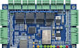
What do you need to start?
PCB photos, scans, Gerbers, or physical board details.
Can you reverse engineer multilayer PCBs?
Yes, including complex multilayer boards.
Are files ready for manufacturing?
Yes, production-ready Gerber and drill files.
Do you sign NDA?
Yes, confidentiality is guaranteed.


