Browse categories
Explore
Fiverr Pro
English
$
USD
PCB DESIGN
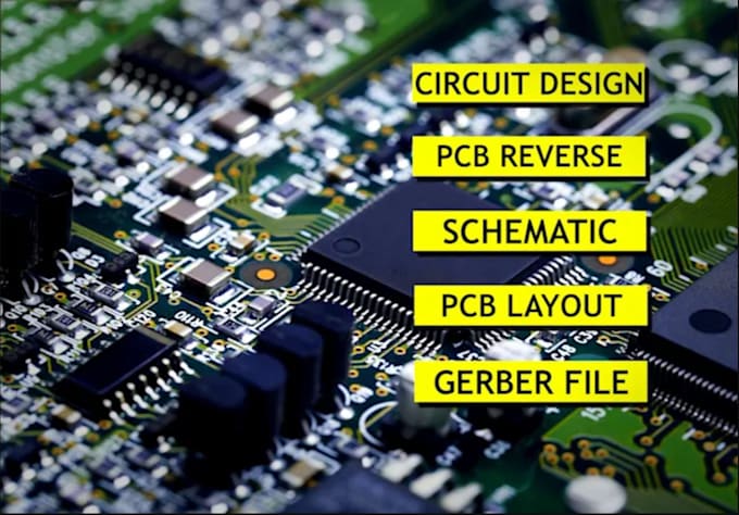
I will do PCB layout design, electronics development and reverse engineering
I will provide PCB layout design, electronics development, circuit de sign, and reverse engineering services for prototypes and production-ready products.
Services Include:
Whether you need a new des1gn, PCB modification, or reverse engineering of an existing board, I will deliver reliable and professional results.
Why Choose Me
What PCB software do you use?
I use KiCad, Altium Designer, EasyEDA, and Eagle CAD.
Can you reverse engineer an existing PCB?
Yes, I can recreate schematics and redesign existing PCBs.
What files will I receive?
Gerber files, source files, BOM, Pick & Place files, and PDF documentation.
Can you design multilayer PCBs?
Yes, I design 2-layer, 4-layer, 6-layer, and higher-layer PCBs.
Do you support manufacturing?
Yes, I provide fabrication-ready files for PCB manufacturers.
Can you sign an NDA?
Yes, all projects are kept confidential.
Do you work on ESP32 and STM32 projects?
Yes, I have extensive experience with ESP32, STM32, Arduino, and embedded hardware.
Do you offer revisions?
Yes, revisions are included according to the selected package.
