Browse categories
Explore
Fiverr Pro
English
$
USD
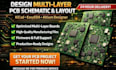
Professional PCB Design and Development Engineer IoT, ESP32, Arduino Expert
Struggling to turn your PCB idea into a fully functional, production-ready de-sign? I specialize in designing multi-layer PCB schematics and layouts that are precise, manufacturable, and optimized for performance.
What I Offer:
I provide end-to-end PCB development using KiCad, EasyEDA, and Altium Designer, including:
Why Choose Me:
Outcome You Get:
A ready-to-manufacture PCB design that meets your exact specifications, reduces errors, and saves cost on prototyping. Whether its a prototype or full production, I ensure your project works flawlessly.
Don't risk your project with inexperienced designers contact me now and get a high-quality, production-ready PCB design delivered within 24 hours


What tools do you use for PCB design?
I work with KiCad, EasyEDA, and Altium Designer, ensuring your PCB is designed with industry-standard software for maximum reliability and manufacturability.
Can you design multi-layer PCBs?
Yes! I specialize in multi-layer PCB schematic and layout design, including signal integrity, power planes, and IoT/ESP32/Arduino integration.
Will I get Gerber files and BOM files?
Absolutely. Every order includes Gerber files, BOM files, and assembly instructions, so your PCB is ready for manufacturing without delays.
Do you provide firmware or software support?
Yes, I offer firmware guidance and integration for IoT, Arduino, and ESP32 systems, ensuring your PCB works seamlessly with your code.
How fast can you deliver?
I can deliver urgent projects within 24 hours for high-priority designs. Standard timelines depend on complexity but are always optimized for quality.


