I will design pcb layout and circuit schematics with gerber, bom in kicad or altium pcb

United States

I speak English, French, German, Spanish, Dutch, Portuguese, Italian

3 orders completed

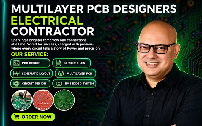
Optimized PCB Layouts for Peak Performance

Hello, I’m Kevin, an Electronics and PCB Design Engineer with hands-on experience in developing reliable, production-ready hardware solutions. I specialize in PCB design, circuit schematics, and embed...
About this Gig

Advanced PCB Design & Electronics Engineering Services | Reliable, Production-Ready Solutions


I'm a professional Electronics and Electrical Design Engineer offering high-quality PCB design services tailored to meet your exact project requirements. With strong expertise in embedded systems, hardware prototyping, circuit design, and PCB layout development, I create efficient, industry-standard designs for a wide range of applications including microcontroller-based systems, RF circuits, and general electronics.


Services Offered:

  • Custom Circuit Schematic Design
  • Professional PCB Layout (26 layers)
  • Gerber Files for Manufacturing
  • Bill of Materials (BOM) with components
  • Pick and Place (Centroid) Files
  • Assembly Layout Documentation
  • 3D PCB Models for Visualization


Technical Capabilities:

  • Support for both THT and SMT components
  • Rigid and Flex PCB design
  • Flexible board shapes, sizes, and dimensions
  • RF and impedance-controlled routing


Software Expertise:

  • EasyEDA
  • Autodesk EAGLE
  • Fusion 360
  • KiCad
  • E EDA


Important Note:

Every project is different, and pricing may vary depending on complexity and requirements. Feel free to reach out before placing an order

Specialization:

Circuit design

Schematics

Layout

Footprint

File format:

Gerber

STEP

SCH

3DS

PDF

Software:

Altium Designer

EasyEDA

KiCad

Proteus

Arduino

Interface:

HDMI

MIPI DSI/CSI

I2S

TDM

UART

USB

SPI

I2C

SDIO

PCIe

Wi-Fi

BT