I will provide complete pcb design, schematic capture, layout, and manufacturing files

Poland

I speak English, Spanish, French

PCB design layout engineer

With over four years of expertise in Electronics Engineering, I bring a unique combination of passion and professionalism to every project. Specializing in PCB design and firmware development, I deliv...
About this Gig

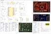
Are you looking for a professional PCB design that is reliable, clean, and ready for manufacturing? You're in the right place.

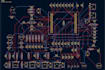
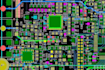
I am an Electrical and Electronics Engineer with hands-on experience in PCB schematic design and PCB layout using KiCad, Altium Designer, and EasyEDA. I design PCBs that are optimized for manufacturability, signal integrity, and power reliability.


What I offer:

  • Complete PCB schematic design
  • Professional PCB layout (single-layer to multi-layer)
  • Design optimized for JLCPCB, PCBWay, Seeed Studio
  • DRC/ERC error-free design
  • Component selection support
  • Manufacturing-ready Gerber files
  • BOM and pick-and-place files
  • Clear documentation and revisions


Applications:

  • Microcontroller & ESP32 boards
  • IoT and embedded systems
  • Power supply and LED driver circuits
  • Sensor and analog/digital PCBs


I focus on clean routing, proper grounding, power integrity, and EMI best practices to ensure your board works as expected on the first fabrication.


Message me before ordering to discuss your project requirements and get the best results.

Specialization:

Circuit design

Schematics

Layout

Footprint

File format:

Gerber

STEP

SCH

3DS

PDF

Software:

Altium Designer

EasyEDA

KiCad

AutoCAD

SolidWorks

Interface:

HDMI

MIPI DSI/CSI

I2S

TDM

UART

USB

SPI

I2C

SDIO

Wi-Fi

BLE