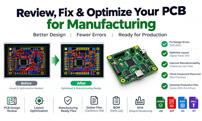
I review, debug and optimize existing PCB designs before fabrication or assembly, focusing on issues that can cause failed prototypes, unstable hardware, manufacturing rejection or unnecessary production cost. I can audit your schematic, PCB layout, BOM & Gerber package against component datasheets, electrical requirements & your manufacturers design rules.
WHAT I REVIEW & FIX
- Schematic errors, ERC warnings & missing connections
- Pinouts, footprints, polarity & component orientation
- Placement, routing, vias, clearances & copper pours
- Power rails, grounding, decoupling & protection
- High-current paths, thermal issues & voltage clearances
- USB, CAN, SPI, I2C, UART & differential signals
- Connectors, test points & mechanical constraints
PRODUCTION OPTIMIZATION
- DRC + manufacturer-specific rule verification
- EMI-aware routing & signal separation
- Trace width, via size & current-capacity checks
- Solder mask, paste, silkscreen & courtyard cleanup
- DFM/DFA review for SMT/THT assembly
- BOM, Gerber, drill & layer-stack verification
DELIVERABLES
- Corrected schematic + PCB source files
- Updated Gerber + NC Drill package
- BOM + Pick-and-Place/Centroid files
- Issue/fix report
Contact me before ordering