Browse categories
Explore
Fiverr Pro
English
$
USD
Firmware Development Embedded Systems Specialist
HELLO AND WELCOME TO MY GIG!!!
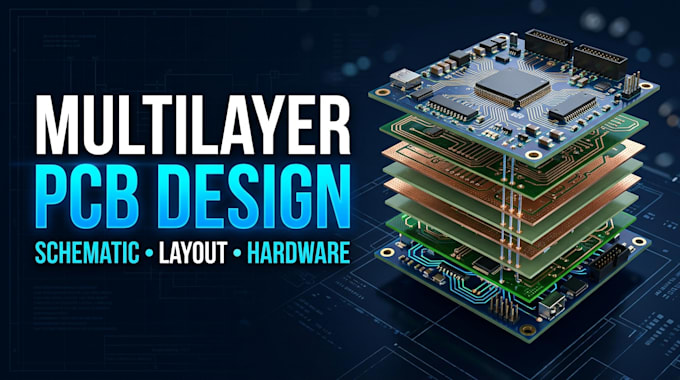
Multilayer PCB design, schematic capture, circuit development, and hardware engineering for reliable electronic products. Specialized in complex PCB layouts, component placement, routing optimization, stackup planning, and manufacturing-ready designs.
WHAT I OFFER;
WHY CHOOSE ME;
Kindly provide your circuit requirements, layer count, board dimensions, components, reference files, and preferred design software.
MESSAGE ME NOW to discuss your multilayer PCB project!
What types of IoT PCB can you design?
I can design PCBs for smart home devices, wireless sensor nodes, industrial monitoring, automation systems, portable electronics, and other connected devices.
Which microcontrollers and modules do you support?
I can work with ESP32, ESP8266, STM32, and other suitable microcontrollers or wireless modules, depending on the project requirements.