Browse categories
Explore
Fiverr Pro
English
$
USD
professional PCB and RF hardware design engineer
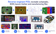
Are you looking to reverse engineer an existing PCB but dont have the original schematic, PCB files, BOM, or Gerbers?
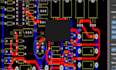
I can help recreate your PCB from a physical board, images, or available documentation. I can trace connections, identify components, recreate the schematic and PCB layout, prepare the BOM, and generate manufacturing-ready Gerber files.
This is ideal for legacy, obsolete, damaged, discontinued, prototype, and replacement PCBs that need to be documented, reproduced, repaired, or redesigned.
You will receive clean and organized design files suitable for further development or manufacturing
What i offer
What You Will Get
CONTACT ME NOW BEFORE PLACING YOUR ORDER!!
What do you need to start the PCB reverse engineering
Please send clear PCB photos, board dimensions, component details, and any available files.
Can you recreate a schematic from a physical PCB
Yes. I can trace the PCB connections and recreate the schematic and component information.
Can you provide manufacturing-ready Gerber files
Yes. Depending on the project, I can provide Gerbers, BOM, drill files, and source design files.
Can you reverse engineer obsolete or damaged PCBs
Yes. I can work with legacy, discontinued, damaged, and prototype boards where the design files are missing.


