Browse categories
Explore
Fiverr Pro
English
$
USD
Electronics Hardware Design Engineer
Struggling with signal loss, poor range, or EMI issues in your RF or telecom project?
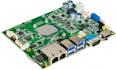
I specialize in professional RF and Telecommunication PCB design for modern wireless applications including 5G, WiFi 6/7, Bluetooth, LoRa, GNSS, radar, microwave, and high-speed communication systems.
I deliver high-performance layouts with excellent signal integrity, minimal loss, and reliable real-world performance even at GHz frequencies.
What You Get:
Software Used:
Message me your project details today Ill provide a quick quote and realistic timeline.

What kind of RF and telecommunication PCBs do you design?
I specialize in RF, high-frequency, and telecommunication PCBs for 5G, WiFi 6/7, Bluetooth, LoRa, GNSS, radar, microwave, and wireless communication systems.
Do you handle antenna design and high-frequency layouts?
Yes. I provide full custom antenna design, tuning, matching networks, controlled impedance routing, and high-frequency material selection (Rogers, Megtron, etc.).
Which software do you use for RF PCB design?
I primarily use Altium Designer (industry standard for RF work) and KiCad. I deliver native source files in your preferred software.
What files will I receive after the project?
You’ll receive complete manufacturing files: Gerber RS-274X, drill files, pick & place, detailed BOM, 3D STEP model, and fabrication notes.
How long does it take to complete an RF or telecom PCB design?
Simple RF projects: 6–8 days Standard 5G/wireless projects: 8–12 days Complex/high-frequency designs: 12–16 days Rush delivery is available.
