Browse categories
Explore
Fiverr Pro
English
$
USD
Is your prototype ready for the factory, or will it fail on the assembly line?
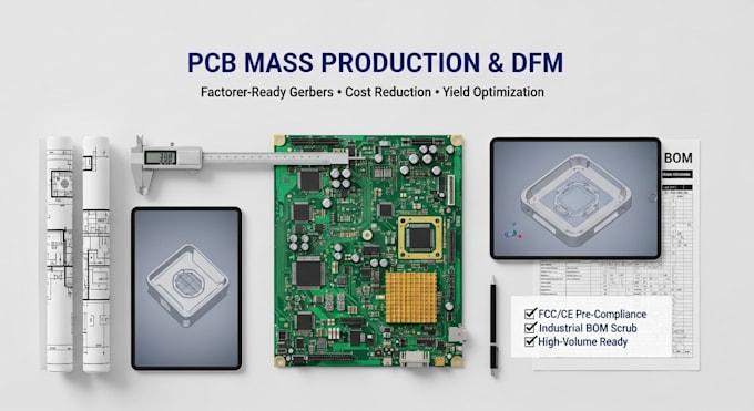
Taking a project from "one working unit" to 1,000 units is the most dangerous stage of product development. Small errors in component spacing, pad sizes, or trace routing can lead to high failure rates and wasted thousands in manufacturing costs.
I am a DFM (Design for Manufacturing) Specialist. I take your existing PCB layouts and optimize them for high-yield, low-cost mass production. I don't just "fix" boards; I ensure they are reliable, scalable, and factory-ready.
What I Solve for You:


File format:
Gerber
•
BRD
•
SCH
•
•
ODB
Software:
Allegro
•
Altium Designer
•
Eagle CAD
•
KiCad
•
Powersim
•
AutoCAD
Interface:
HDMI
•
MIPI DSI/CSI
•
Wi-Fi
•
BLE
•
CAT-M1
•
Ethernet
Can you help me lower my unit cost?
Yes. Part of my DFM process is a "BOM scrub" where I identify expensive or "end-of-life" parts and replace them with cost-effective, long-term alternatives.
Do you communicate with the factory?
Absolutely. I can act as your technical liaison with fab houses like PCBWay or Tier-1 manufacturers to resolve any technical queries during the build.
Can you design a test fixture?
Yes, the Premium package includes the design of a specialized test jig (Bed-of-Nails) to ensure every unit leaving the factory is 100% functional.