I will develop pcb schematics and layouts with industry standards

United Kingdom

I speak English

pcb

I am a PCB designer who focuses on building designs that work beyond the schematic. I don’t just place components and route traces—I analyze how each part interacts within the system, ensuring stabili...
About this Gig

HELLO BUYER

WELCOM!!

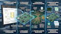
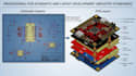
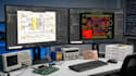
I specialize in developing high fidelity PCB schematics and layouts that bridge the gap between a prototype and a market ready product. My process is rooted in industry rigor ensuring that every net is calculated, every component is sourceable, and every board is optimized for 100% yield at the factory. Whether you are building an industrial IoT gateway or a high-speed medical device, I provide the technical backbone your hardware needs to perform flawlessly under pressure.

what i offer

  • Professional Schematic Capture
  • High Speed Layout Engineering
  • Industrial Stack up Design
  • Manufacturing Ready File Vault
  • Smart Sourcing and BOM Management
  • Mechanical Master Fit (3D STEP)
  • DFM and DFA Optimization

why choose me

  • The Zero Respin Objective
  • Manual Precision
  • Software Agnostic Expertise
  • EMI/EMC-Centric Thinking
  • End to End Partnership

Ready to Engineer Your Success.

message me now for your project before placing an order

Specialization:

Circuit design

Schematics

Layout

Footprint

File format:

Gerber

STEP

3DS

PDF

ODB

Software:

Altium Designer

Eagle CAD

EasyEDA

KiCad

LTspice

Matlab

Interface:

HDMI

MIPI DSI/CSI

I2S

TDM

UART

USB

SPI

I2C

SDIO

PCIe

Wi-Fi

BLE