Browse categories
Explore
Fiverr Pro
English
$
USD
pcb design and enclosure design
HELLO AND WELCOME!
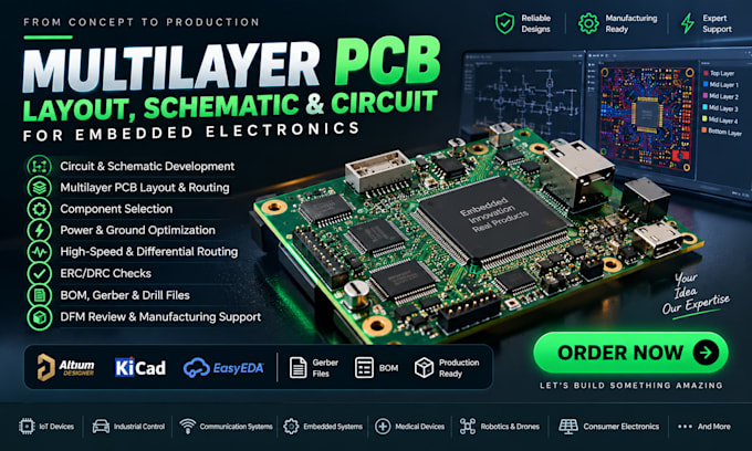
Need a reliable PCB solution for your embedded electronics project? I can help turn your circuit concept, requirements, or existing schematic into a practical, manufacturing-ready board.
My services include:
What sets me apart:
I focus on clean routing, logical component placement, manufacturability, signal integrity, and reliable power distributionnot just making the board look complete. I also communicate clearly throughout the project to reduce costly revisions.
Whether you're developing an IoT device, industrial controller, embedded system, sensor board, or custom electronics, I can help you move from concept to production-ready PCB files.
Send me your requirements today and let's turn your electronics idea into a reliable PCB solution.

Specialization:
Circuit design
•
Schematics
•
Layout
File format:
Gerber
•
BRD
•
Software:
Altium Designer
•
Eagle CAD
Interface:
UART
•
USB
•
I2C
Can you work from an existing schematic?
Yes. I can create the PCB layout from your schematic or review and improve an existing design.
Do you support multilayer PCBs?
Yes. I can handle 2-layer, 4-layer, 6-layer, and more complex multilayer boards.
What PCB software do you use?
I can work with KiCad, Altium Designer, and other common PCB design tools.
. Can you handle high-speed routing?
Yes. High-speed and differential-pair routing can be included depending on the project requirements.
