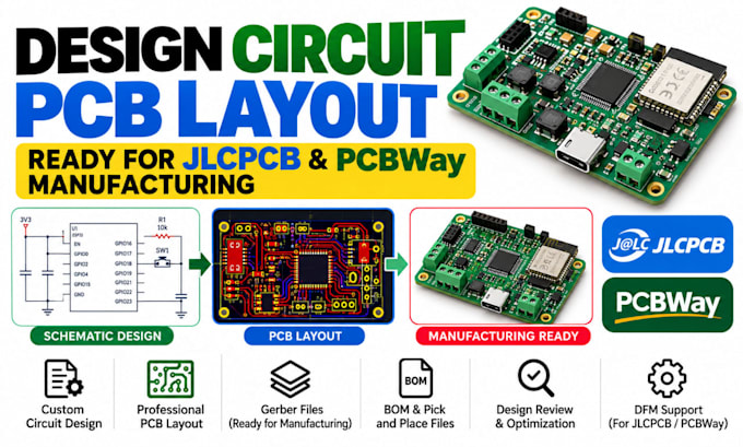
I design custom circuits, PCB schematics and PCB layouts that are fully ready for JLCPCB and PCBWay manufacturing and assembly. I can work from your idea, block diagram, datasheets, breadboard, prototype or existing schematic to deliver clean, manufacturable boards.
WHAT I OFFER
- Custom circuit design & schematic capture
- Single, double & multilayer PCB layout
- Component selection, footprints & library creation
- MCU, IoT, sensor, power, control & embedded boards
- UART, SPI, I2C, USB, CAN, RS485 & other interfaces
- ERC/DRC verification with manufacturer design rules
MANUFACTURING OPTIMIZATION
- JLCPCB & PCBWay-compliant clearances, vias & drill sizes
- Ground planes, decoupling & power distribution
- Current-rated trace widths, copper pours & thermal relief
- EMI-aware routing & differential pairs where required
- DFM/DFA checks for SMT/THT assembly
- Solder mask, paste, silkscreen, test points & mounting holes
DELIVERABLES
- Editable schematic + source files
- Gerber + NC Drill files
- BOM with manufacturer part numbers
- Pick-and-Place/Centroid files
- PDF schematic & assembly references
- Optional STEP/3D PCB model
NDA available. Contact me before ordering with your circuit requirements, board dimensions.