Browse categories
Explore
Fiverr Pro
English
$
USD
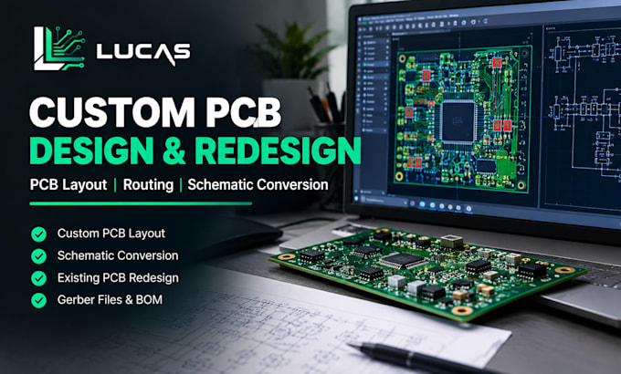
Professional PCB Design, Reliable, Manufacturable Circuit Board Solutions
Looking for a professional PCB design that is accurate, organized, and ready for manufacturing? Im Lucas, a PCB design specialist helping individuals, startups, engineers, and businesses turn electronic concepts into functional circuit board.
My Services Include:
Why work with me?
Whether you're developing a prototype, upgrading an existing circuit, or preparing a new electronic product, I'm ready to help.
Let's bring your electronics project to life!
Contact me before ordering complex projects to discuss your requirements and ensure the right solution.
1. Can you convert my schematic into a PCB layout?
Yes. I can help convert your supplied schematic into an organized PCB layout based on your design requirements.
2. Can you redesign an existing PCB?
Yes. I can help modify existing layouts, improve component placement, and optimize routing according to your specifications.
3. Do you support multilayer PCB designs?
Yes. I accept suitable multilayer PCB projects depending on their complexity and technical requirements.
4. Can you work with my preferred PCB software?
Please contact me with your preferred software and file format so I can confirm compatibility before ordering.
