Browse categories
Explore
Fiverr Pro
English
$
USD
PCB Designer
Need a reliable circuit and PCB layout expert for your electronics project?
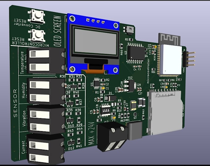
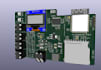
I am a professional PCB designer and electrical engineer with real hands-on project experience using KiCad. and also deliver complete manufacture-ready PCB from schematic to Gerber files for startups, entrepreneurs, and product developers worldwide.
what i mainly do is
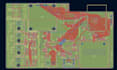
Every layout is optimized for signal integrity, power electronics, and clean routing. I also perform full DRC and pcb review before delivery to catch every error.
You will receive everything:
Fast delivery,with clear communication, and revisions until you are 100% satisfied are guaranteed. Send me your circuit idea, hand sketch, or partial schematic and I will turn it into a professional, production-ready PCB.
Message me now and let's bring your electronics design to life!


Specialization:
Circuit design
•
Schematics
•
Layout
•
Footprint
•
Gerber
File format:
Gerber
•
STEP
•
SCH
•
3DS
•
Software:
KiCad
•
LTspice
Interface:
HDMI
•
I2S
•
UART
•
Wi-Fi
What files will I receive?
Gerber files, Schematic PDF, BOM, and 3D model (Premium only)
Which software do you use?
KiCad
Can you work from my hand sketch?
Yes. Just send a photo or PDF.
Will the PCB be ready for manufacturing?
Yes. Files are JLCPCB/PCBWay compatible.
How many revisions do I get?
2 free revisions per order.
Do you provide component purchase links?
Yes, with the $10 extra service
What if I need more than 25 components?
Contact me for custom quote.