Browse categories
Explore
Fiverr Pro
English
$
USD
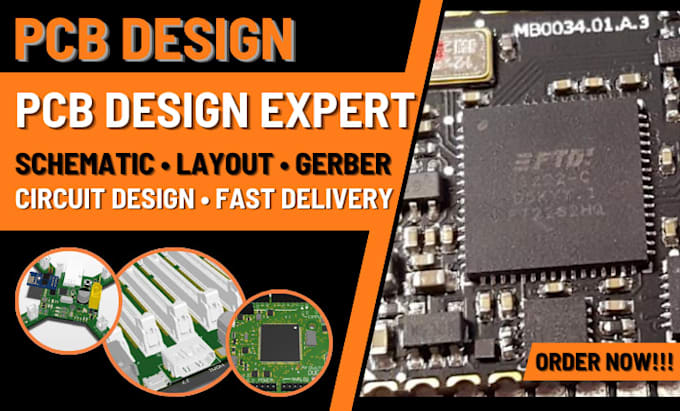
PCB Design Expert, Altium, KiCad, ESP32, Arduino And IoT
Are you looking for a professional PCB design that is clean, optimized, and ready for manufacturing? Youre in the right place.
I am a PCB design specialist with experience in circuit design, embedded systems, and product development. I help turn ideas, sketches, or requirements into high-quality PCB layouts that are optimized for performance and real-world applications.
With strong expertise in schematic design and PCB layout, I ensure proper routing, component placement, and manufacturability so your project works perfectly after fabrication.
I can help you with:
You will receive:
Software I use:
Every project is unique, so feel free to contact me before placing your order. I will review your project and provide the best solution.


File format:
Gerber
•
STEP
•
BRD
•
SCH
•
Software:
Eagle CAD
•
EasyEDA
•
Fusion 360
•
KiCad
•
AutoCAD
Interface:
I2S
•
UART
•
USB
•
SPI
•
I2C
•
BT
•
GSM/GPRS
•
LTE
Can you design PCB from scratch?
Yes, I can design both schematic and PCB from your idea.
Are the files ready for manufacturing?
Yes, you will receive fully production-ready files.
What if I already have a schematic?
What if I already have a schematic?
Do you redesign or fix PCB issues?
Yes, I can optimize and fix existing designs.
How do I know which package to choose?
Message me and I will guide you based on your project.