Browse categories
Explore
Fiverr Pro
English
$
USD
Level 1
Has met certain performance criteria and shows strong potential in the marketplace.
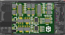
I will professionally design electronic circuits and PCB layouts and deliver manufacturing-ready Gerber and BOM files for your project.
This gig covers the complete PCB design workflow, from concept to production. Whether you have an idea, block diagram, or reference design, I will convert it into a reliable and clean PCB layout that meets industry standards.
What I offer:
Suitable for:
Arduino, ESP32, STM32, power supplies, sensor boards, IoT devices, and general electronics projects.
I focus on signal integrity, manufacturability, and clean routing to ensure your board works perfectly on first production.
If you are unsure which package to choose, contact me before ordering.

What software do you use?
KiCad / EasyEDA / Altium (as required).
Can you design from an idea only?
Yes, a block diagram or description is enough.
Will files be ready for manufacturing?
Yes, all outputs are fabrication-ready.
Do you support PCB manufacturers?
Yes, JLCPCB, PCBWay, and others.
Can you fix or redesign existing PCB?
Yes, just share your files.
