Browse categories
Explore
Fiverr Pro
English
$
USD
PCB ELECTRICAL ENGINEER EXPERT
HELLO AND WELCOME TO MY GIG!!!
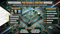
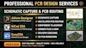
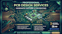
I will do professional schematic capture and PCB routing in Altium Designer, KiCad, and EasyEDA for electronic, embedded, IoT, automotive, and industrial projects. Whether you need a simple PCB, multilayer board, STM32 system, or manufacturing ready layout, I will deliver clean, optimized, and reliable PCB solutions tailored to your requirements.
My service focuses on accurate schematic development, efficient routing, signal integrity, proper component placement, and fabrication ready outputs to ensure smooth PCB manufacturing and performance.
What I Offer
Why Choose Me
Please message me before placing your order to discuss your schematic capture and PCB routing project in Altium, KiCad, or EasyEDA professionally!!!
Which PCB software do you support?
Altium Designer, KiCad, EasyEDA, and more.
Do you provide Gerber files?
Yes, manufacturing ready files are included.
Can you design multilayer PCBs?
Yes, including advanced routing projects.
Do you support schematic capture?
Yes, schematic and PCB routing are included.
Can you optimize routing and placement?
Yes, for performance and manufacturability.


