Browse categories
Explore
Fiverr Pro
English
$
USD
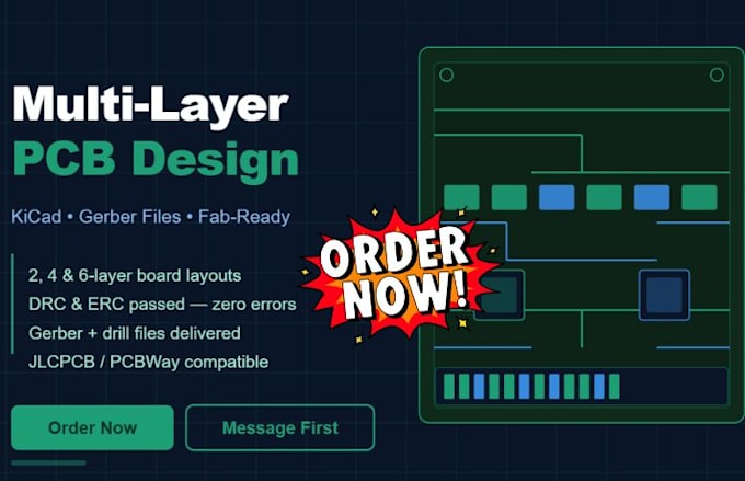
Precision PCB Design That Works First Time
Most PCB designers give you a layout that looks fine on screen but causes real headaches at the fab house wrong layer stack, missing drill files, DRC errors you only discover after paying for a prototype.
I use KiCad to design multi-layer PCBs that are clean, accurate, and manufactured without problems the first time.
What you get:
I've designed boards for IoT devices, power electronics, microcontroller modules, sensor arrays, and embedded systems.
Message me before ordering, share your schematic or describe your project and I'll let you know exactly what layer count and approach makes sense.


Specialization:
Circuit design
•
Schematics
•
Layout
•
Gerber
File format:
Gerber
Software:
Altium Designer
•
EasyEDA
•
KiCad
Why multi-layer instead of 2-layer?
When component density is high, signal integrity matters, or you need dedicated power and ground planes, multi-layer is the cleaner, more reliable solution. I'll advise you on the right choice for your project.
What do I need to provide?
A schematic (KiCad, EasyEDA, PDF, or image) plus any mechanical constraints like board size or connector positions. The more info you give, the better the result.
Which fab houses are your Gerbers compatible with?
JLCPCB, PCBWay, OSHPark, Seeed Studio, and any standard fab house that accepts Gerber RS-274X format.
Can you design the schematic too?
Yes, message me to discuss. Schematic design can be added as an extra or included in a custom offer.
Do I get the KiCad source files?
Yes, always. You'll own the full project files and can edit them anytime without needing proprietary software.
What if the board has issues at the fab house?
Every delivery is DRC-clean, so fab issues from my side are extremely rare. If something goes wrong due to my design, I'll fix it immediately at no cost.