Browse categories
Explore
Fiverr Pro
English
$
USD
Electronics Hardware Design Engineer
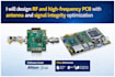
Are you looking for a high-performance RF PCB deslgn that ensures clean signals, low loss, and reliable operation at high frequencies? I specialize in RF, microwave, and high-speed PCB deslgn focused on signal integrity, impedance control, and antenna optimization for modern electronic systems.
I design PCB layouts for wireless communication, IoT devices, telecom hardware, 5G circuits, radar systems, and other high-frequency applications where precision is critical.
My expertise includes RF PCB layout deslgn, controlled impedance routing (50Ω/75Ω), stack-up delign, transmission line design, proper grounding techniques, and EMI/EMC reduction strategies. I also ensure efficient antenna integration for maximum performance and minimal interference. Every deslgn is optimized for manufacturability (DFM/DFA) and real-world reliability.
I use industry-standard tools like Altium Deslgner and KiCad to deliver professional, production-ready files.
Whether you need a new RF PCB deslgn or optimization of an existing high-speed circuit, I can help you achieve stable, high-quality, and industry-compliant results.
What information do you need to start the RF PCB design?
I need your schematic (or idea), required frequency range, number of layers, board size, component list, and any special requirements such as impedance control, antenna type, or constraints. If you only have an idea, I can help you develop it into a complete RF PCB design.
Can you work on high-frequency and RF designs like 5G, IoT, or microwave circuits?
Yes. I specialize in RF, microwave, and high-speed PCB designs used in 5G systems, IoT devices, wireless communication, radar, and telecom applications. I ensure proper signal integrity, impedance matching, and EMI/EMC control for high-frequency performance.
Do you ensure signal integrity and impedance control in your designs?
Absolutely. I apply controlled impedance routing (50Ω / 75Ω), proper stack-up design, grounding techniques, and transmission line theory to ensure clean signal flow, minimal loss, and stable high-frequency operation.
What files will I receive after the PCB design is completed?
You will receive complete production-ready files including Gerber files, BOM (Bill of Materials), PCB layout files, stack-up details, and assembly documentation if required. Everything is prepared for direct manufacturing.
Which tools do you use for RF PCB design?
I use industry-standard PCB design tools such as Altium Designer and KiCad. These tools allow me to deliver professional, accurate, and manufacturable RF and high-speed PCB layouts.


