Browse categories
Explore
Fiverr Pro
English
$
USD
I will g0ogle autocomplete website ranking, google autocomplete for keyword firs
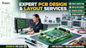
A poorly designed PCB costs time, money, and production runs. I deliver accurate, manufacturing-ready PCB designs and schematics in KiCad done right the first time.
I transform your concept, datasheet, or rough idea into a fully optimized, fabrication-ready circuit board, from simple prototypes to complex multi-layer systems.
What I Offer
Why Clients Choose Me
Deliverables
I deliver reliable, production-ready designs across IoT, power electronics, audio, sensors, and embedded systems.

Do you handle both schematic and PCB layout, or just one?
I handle both starting from your concept or datasheet through to a complete, fabrication-ready PCB layout.
How long does a project take
Most standard designs are completed within a few days; timeline confirmed after reviewing your requirements.
Is my design guaranteed to pass DRC and be manufacturable
Every design goes through Design Rule Check (DRC) verification and is checked for manufacturability before delivery.
