Browse categories
English
$
USD
Connect to your AI
Electronics Engineering Student
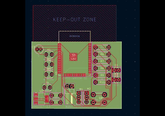
Welcome to my Professional PCB Design and Schematic Layout Service!
Are you looking for a reliable hardware design engineer to transform your circuit idea, block diagram, or schematic into a production-ready Printed Circuit Board (PCB)? You are in the right place!
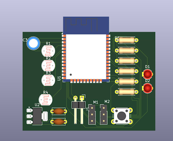
I specialize in designing high-quality, reliable, and manufacturing-ready PCB layouts using KiCad and AutoCAD. Whether you need a simple single-layer board or a complex multi-layer PCB, I deliver designs optimized for fabrication and assembly (JLCPCB, PCBWay, etc.).
What I Offer:
Deliverables Included in Every Order:


File format:
Gerber
•
SCH
•
3DS
•
•
Pcbdoc
Software:
Eagle CAD
•
KiCad
Interface:
USB
•
SPI
•
I2C
What details or files do I need to provide to get started?
You can provide a schematic diagram, hand-drawn circuit sketch, component list, or a clear description of your project along with board size constraints.
Will I receive manufacturing-ready files for JLCPCB, PCBWay, or Altium/KiCad fabrication?
Yes, I will provide complete Gerber files (RS-274X), NC Drill files, BOM, and Pick & Place files formatted specifically for seamless fabrication and assembly.
What software do you use for PCB layout and schematics?
I primarily use KiCad and AutoCAD for precise schematic capture, PCB routing, and mechanical/enclosure dimensions.
Can you provide 3D models of the finished PCB?
Yes, I deliver 3D STEP/VRML models so you can check mechanical alignment and enclosure fitment before ordering fabrication.