Browse categories
Explore
Fiverr Pro
English
$
USD
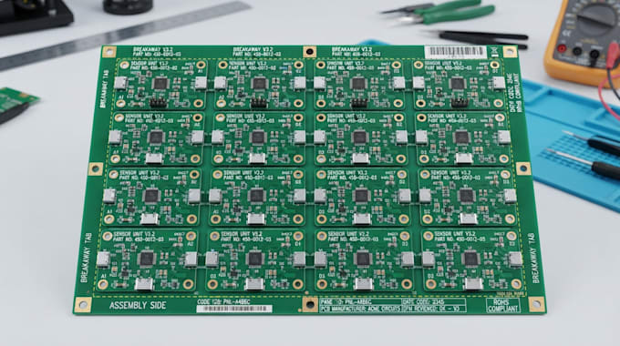
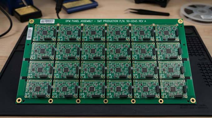
High-speed digital buses and radio frequency links instantly degrade if your multi-layer stackup neglects precise impedance matching and clean return paths. If your hardware prototype exhibits unexpected data corruption, wireless dropouts, or just failed official regulatory lab emissions tests, your layout is suffering from severe electromagnetic interference or trace-to-trace crosstalk.
I provide advanced hardware intervention to diagnose, shield, and eliminate signal integrity and EMI/EMC compliance issues within your current PCB layout. Your board will undergo comprehensive return path tracing, differential pair validation, and power plane optimization to silence background noise. By restructuring layer configurations and correcting termination resistor placement, I pull your design into strict compliance.
You receive optimized, production-ready Gerber archives, updated layout source documents, and precise stackup parameters.
Let's clear your signal noise. Kndly inbox me your layout archives and lab test failure logs before ordering.
How do you fix crosstalk issues on an existing high-density layout?
I isolate parallel traces by enforcing the 3W spacing rule and inserting ground isolation traces. If layers permit, I reroute conflicting high-speed lines orthogonally across adjacent routing levels to eliminate mutual inductive coupling entirely
Can you fix a board that failed FCC or CE electromagnetic emissions testing?
Yes. I analyze the specific failing frequencies from your lab report, then optimize your decoupling capacitor placement, re-engineer your return paths, and introduce via stitching or physical shielding to suppress radiation.
What parameters do you check to ensure proper signal integrity?
I audit differential pair impedance matching, trace length tolerances for timing skew, reference plane discontinuity, power plane resonance, and switching noise. This guarantees clean eye-diagram performance on high-speed buses.
Will you modify my schematic symbols or just the physical board traces?
I primarily fix physical traces and layer stackups. However, if the issue stems from missing termination resistors or insufficient power filtering capacitors, I will update your schematic to accurately reflect those critical hardware changes.